Chih-Yi Cheng, Wei-Liang Pai, Yi-Hsun Chen, Naomi Tabudlong Paylaga, Pin-Yun Wu, Chun-Wei Chen, Chi-Te Liang, Fang-Cheng Chou, Raman Sankar, Michael S. Fuhrer, Shao-Yu Chen*, and Wei-Hua Wang*
Nano Lett., 22, 6, 2270–2276 (2022).

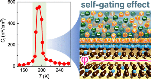
Understanding the Coulomb interactions between two-dimensional (2D) materials and adjacent ions/impurities is essential to realizing 2D material-based hybrid devices. Electrostatic gating via ionic liquids (ILs) has been employed to study the properties of 2D materials. However, the intrinsic interactions between 2D materials and ILs are rarely addressed. This work studies the intersystem Coulomb interactions in IL-functionalized InSe field-effect transistors by displacement current measurements. We uncover a strong self-gating effect that yields a 50-fold enhancement in interfacial capacitance, reaching 550 nF/cm2 in the maximum. Moreover, we reveal the IL-phase-dependent transport characteristics, including the channel current, carrier mobility, and density, substantiating the self-gating at the InSe/IL interface. The dominance of self-gating in the rubber phase is attributed to the correlation between the intra- and intersystem Coulomb interactions, further confirmed by Raman spectroscopy. This study provides insights into the capacitive coupling at the InSe/IL interface, paving the way to developing liquid/2D material hybrid devices.
Yi-Hsun Chen, Chih-Yi Cheng, Shao-Yu Chen, Jan Sebastian Dominic Rodriguez, Han-Ting Liao, Kenji Watanabe, Takashi Taniguchi, Chun-Wei Chen, Raman Sankar, Fang-Cheng Chou, Hsiang-Chih Chiu, and Wei-Hua Wang
npj 2D Materials and Applications, 3 (49) (2019) P. 1

In 2D-semiconductor-based field-effect transistors and optoelectronic devices, metal–semiconductor junctions are one of the crucial factors determining device performance. The Fermi-level (FL) pinning effect, which commonly caused by interfacial gap states, severely limits the tunability of junction characteristics, including barrier height and contact resistance. A tunneling contact scheme has been suggested to address the FL pinning issue in metal–2D-semiconductor junctions, whereas the experimental realization is still elusive. Here, we show that an oxidized-monolayer-enabled tunneling barrier can realize a pronounced FL depinning in indium selenide (InSe) transistors, exhibiting a large pinning factor of 0.5 and a highly modulated Schottky barrier height. The FL depinning can be attributed to the suppression of metal- and disorder-induced gap states as a result of the high-quality tunneling contacts. Structural characterizations indicate uniform and atomically thin surface oxidation layer inherent from nature of van der Waals materials and atomically sharp oxide–2D-semiconductor interfaces. Moreover, by effectively lowering the Schottky barrier height, we achieve an electron mobility of 2160 cm2/Vs and a contact barrier of 65 meV in two-terminal InSe transistors. The realization of strong FL depinning in high-mobility InSe transistors with the oxidized monolayer presents a viable strategy to exploit layered semiconductors in contact engineering for advanced electronics and optoelectronics.
Cheng-Hua Liu, Po-Hsiang Wang, Tak-Pong Woo, Fu-Yu Shih, Shih-Ching Liou, Po-Hsun Ho, Chun-Wei Chen, Chi-Te Liang, and Wei-Hua Wang*
Physical Review B: Rapid Communications 93 (2016) P. 041421(R)

We report distinctive magnetotransport properties of a graphene p-n-p junction prepared by controlled diffusion of metallic contacts. In most cases, materials deposited on a graphene surface introduce substantial carrier scattering, which greatly reduces the high mobility of intrinsic graphene. However, we show that an oxide layer only weakly perturbs the carrier transport, which enables fabrication of a high-quality graphene p-n-p junction through a one-step and resist-free method. The measured conductance-gate voltage curves can be well described by a metal contact model, which confirms the charge density depinning due to the oxide layer. The graphene p-n-p junction samples exhibit pronounced quantum Hall effect, a well-defined transition point of the zeroth Landau level (LL), and scaling behavior. The scaling exponent obtained from the evolution of the zeroth LL width as a function of temperature exhibits a relatively low value of κ=0.21. Moreover, we calculate the energy level for the LLs based on the distribution of plateau-plateau transition points, further validating the assignment of the LL index of the QH plateau-plateau transition.
Yueh-Chun Wu, Cheng-Hua Liu, Shao-Yu Chen, Fu-Yu Shih, Po-Hsun Ho, Chun-Wei Chen, Chi-Te Liang, and Wei-Hua Wang*
Scientific Report, 5 (2015) P. 11472

Recent discoveries of the photoresponse of molybdenum disulfide (MoS2) have shown the considerable potential of these two-dimensional transition metal dichalcogenides for optoelectronic applications. Among the various types of photoresponses of MoS2, persistent photoconductivity (PPC) at different levels has been reported. However, a detailed study of the PPC effect and its mechanism in MoS2 is still not available, despite the importance of this effect on the photoresponse of the material. Here, we present a systematic study of the PPC effect in monolayer MoS2 and conclude that the effect can be attributed to random localized potential fluctuations in the devices. Notably, the potential fluctuations originate from extrinsic sources based on the substrate effect of the PPC. Moreover, we point out a correlation between the PPC effect in MoS2 and the percolation transport behavior of MoS2. We demonstrate a unique and efficient means of controlling the PPC effect in monolayer MoS2, which may offer novel functionalities for MoS2-based optoelectronic applications in the future.
Shao-Yu Chen, Po-Hsun Ho, Ren-Jye Shiue, Chun-Wei Chen*, and Wei-Hua Wang*
Nano Letter,12(2) (2012) P. 964

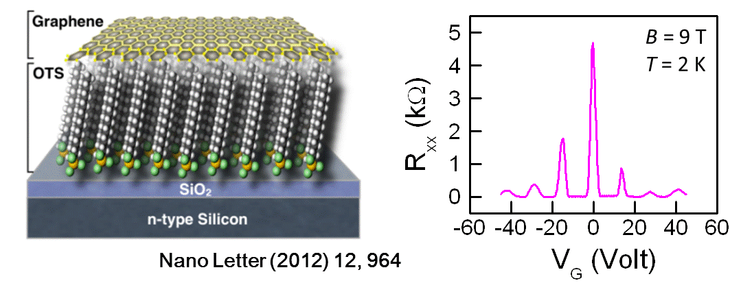
In this article, we present the transport and magnetotransport of high-quality graphene transistors on conventional SiO2/Si substrates by modification with organic molecule octadecyltrichlorosilane (OTS) self-assembled monolayers (SAMs). Graphene devices on OTS SAM-functionalized substrates with high carrier mobility, low intrinsic doping, suppressed carrier scattering, and reduced thermal activation of resistivity at room temperature were observed. Most interestingly, the remarkable magnetotransport of graphene devices with pronounced quantum Hall effect, strong Shubnikov-de Haas oscillations, a nonzero Berry’s phase, and a short carrier scattering time also confirms the high quality of graphene on this ultrasmooth organic SAM-modified platform. The high-performance graphene transistors on the solution-processable OTS SAM-functionalized SiO2/Si substrates are promising for the future development of large-area and low-cost fabrications of graphene-based nanoelectronics.
Hung-Chieh Cheng,§ Ren-Jye Shiue,§ Chia-Chang Tsai, Wei-Hua Wang,* and Yit-Tsong Chen*
ACS Nano, 5 (2011) P. 2051

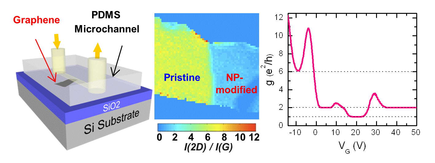
An essential issue in graphene nanoelectronics is to engineer the carrier type and density and still preserve the unique band structure of graphene. We report the realization of high-quality graphene p-n junctions by non-covalent chemical functionalization. A generic scheme for the graphene p-n junction fabrication is established by combining the resist-free approach and spatially-selective chemical modification process. The effectiveness of the chemical functionalization is systematically confirmed by surface topography and potential measurements, spatially-resolved Raman spectroscopic imaging, and transport/magnetotransport measurements. The transport characteristics of graphene p-n junctions are presented with observations of high carrier mobilities, Fermi energy difference, and distinct quantum Hall plateaus. The chemical functionalization of graphene p-n junctions demonstrated in this study is believed to be a feasible scheme for modulating the doping level in graphene for future graphene-based nanoelectronics.
 中央研究院 原子與分子科學研究所

