Heming Yao, Ya-Ping Hsieh, Jing Kong and Mario Hofmann
Nature Materials, 19, 745–751 (2020).

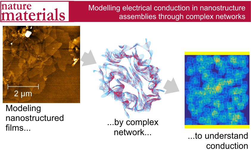
Carrier transport processes in assemblies of nanostructures rely on morphology-dependent and hierarchical conduction mechanisms, whose complexity cannot be captured by current modelling approaches. Here we apply the concept of complex networks to modelling carrier conduction in such systems. The approach permits assignment of arbitrary connectivity and connection strength between assembly constituents and is thus ideal for nanostructured films, composites and other geometries. Modelling of simplified rod-like nanostructures is consistent with analytical solutions, whereas results for more realistic nanostructure assemblies agree with experimental data and reveal conduction behaviour not captured by previous models. Fitting of ensemble measurements also allows the conduction properties of individual constituents to be extracted, which are subsequently used to guide the realization of transparent electrodes with improved performance. A global optimization process was employed to identify geometries and properties with high potential for transparent conductors. Our intuitive discretization approach, combined with a simple solver tool, allows researchers with little computational experience to carry out realistic simulations.
Szu-Hua Chen, Yen Nguyen, Ting-Wei Chen, Zhi-Long Yen, Mario Hofmann, Ya-PingHsieh
Carbon, DOI: doi.org/10.1016/j.carbon.2020.04.036 (2020).

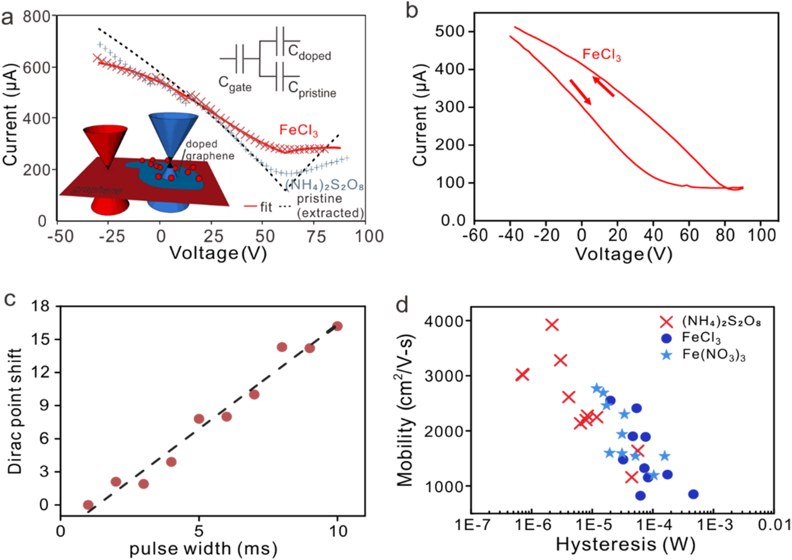
The carrier conduction in 2D materials is more sensitive to surface-bound disorder than bulk materials which is thought to limit their achievable performance in electronic devices. To date, charged impurity scattering is considered the main source of interaction between ionic adsorbates and carriers in 2D materials. We here observe a previously unknown source of carrier scattering in graphene upon interaction with ionic impurities. Different from charged impurity scattering, these “neutral scatterers” do not depend on carrier concentration and result in a sixfold mobility variation at similar doping. Comparison of different ionic residue from various metal etchants reveals a universal mechanism that controls the carrier mean free path. Raman spectroscopy suggests that inhomogeneous charge distribution is the source of neutral scatterers and we extract an optical fingerprint for their presence. The charge heterogeneity thus acts as an additional degree of freedom in graphene's carrier transport and its consideration can explain the transition from ambipolar to unipolar charge transport in graphene. Our results not only provide new insight into the carrier transport of 2D materials in the presence of disorder and provide guidelines for enhancing the performance of graphene devices but also enable novel device concepts in graphene.
Ding-Rui Chen, Mario Hofmann, He-Ming Yao, Sheng-Kuei Chiu, Szu-Hua Chen, Yi-Ru Luo, Chia-Chen Hsu, and Ya-Ping Hsieh*
ACS Applied Materials & Interface 11, 6384-6388 ( 2019).

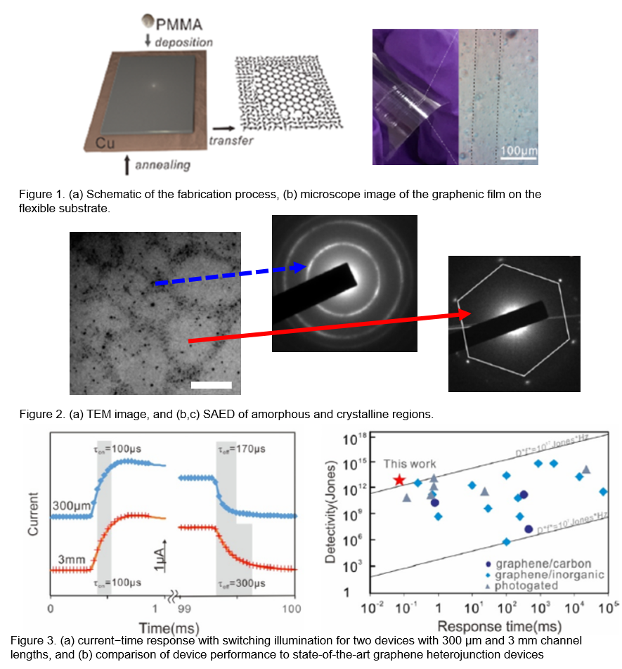
Lateral heterojunctions in two-dimensional (2D) materials have demonstrated potential for high-performance sensors because of the unique electrostatic conditions at the interface. The increased complexity of producing such structures, however, has prevented their widespread use. We here demonstrate the simple and scalable fabrication of heterojunctions by a one-step synthesis process that yields photodetectors with superior device performance. Carrier transport in these heterojunctions was found to proceed by minimizing the path through the amorphous carbon barriers, which results in a self-selective Schottky emission process with high uniformity and low emission barriers. We demonstrate the potential of thus produced heterojunctions by realizing a photodetector that combines an ultrahigh detectivity of 1013 Jones with microsecond response time, which represents the highest performance of 2D material heterojunction devices. These attractive features are retained even for millimeter-scale devices, and the demonstrated ability to produce transparent, patterned, and flexible sensors extends lateral heterojunction sensors toward wearable and large-scale electronics.
H. T. Chin,‡a C. H. Shih,‡a Y. P. Hsieha*, C. C. Tinga, J. N. Aohb and M. Hofmannc
PCCP 2017, Sep
The growth of two-dimensional materials into three-dimensional geometries holds the promise for high performance hybrid materials and novel architectures. The synthesis of such structures, however, proceeds in fundamentally different flow regimes than conventional CVD where pressure differences and wall collisions are neglected. We here demonstrate the remarkable stability of graphene growth under varying fluid dynamical flow regimes. We investigate the growth process across different flow conditions using confined growth in refractory pores. Analysis of the growth rate reveals a transport-limited process which allows experimental determination of the gas diffusion coefficient. The diffusion coefficient was found to be constant for large pore dimension but scales with pore dimension as the pore size decreases below the mean free path providing clear evidence for previously predicted Knudsen molecular-flow conditions for atomic confinement. Surprisingly, changes to the flow conditions by two orders of magnitude do not cause qualitative changes of the graphene growth process. This unique behavior was attributed to rarefied flow conditions by scaling analysis and an analytical relation between growth rate and constriction could be extracted that proves accurate throughout the investigated conditions. Our results demonstrate a fundamentally different growth process compared to traditional CVD processes that is akin to atomic layer deposition and highlight the feasibility of high-quality 2D-material growth on 3D morphologies with ultra-high aspect ratios.
Ya-Ping Hsieh*, Ching-Hua Shih, Yi-Jing Chiu& Mario Hofmann
Chemistry of Materials, 28 (1), 40–43 (2016).

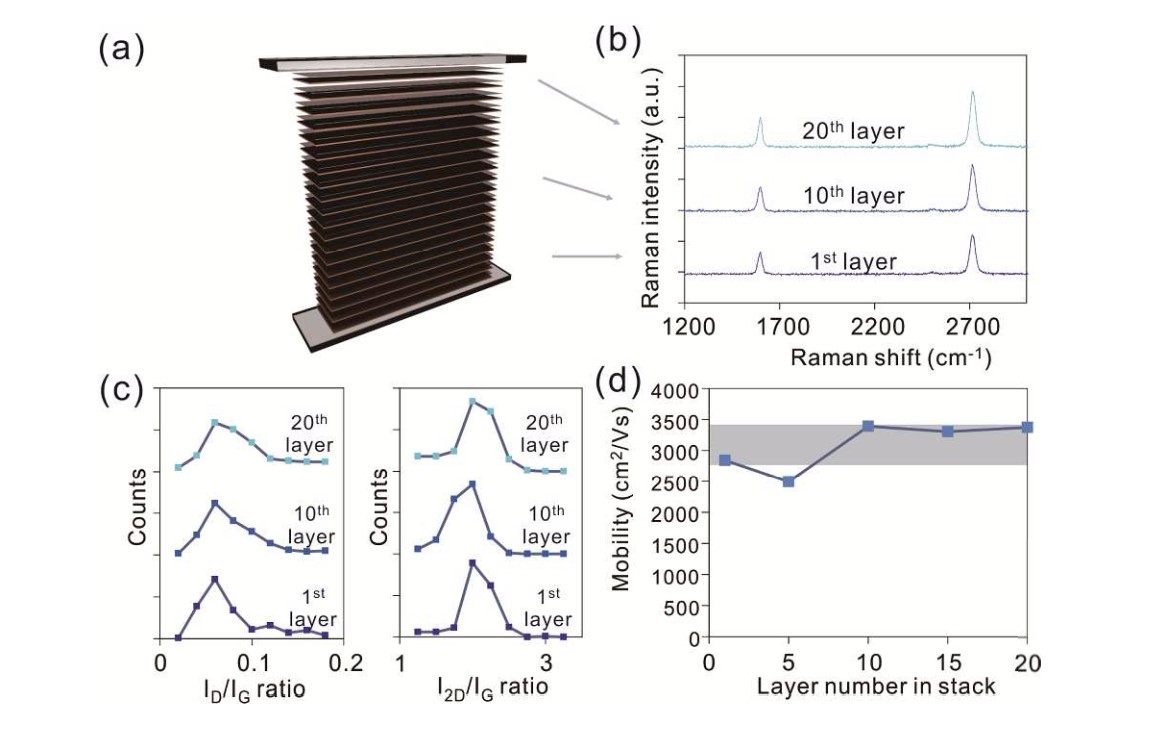
The scalable production of high quality graphene could enable many applications ranging from high-speed electronics to transparent solar cells. While chemical vapor deposition has demonstrated the ability to produce graphene with suitable properties the scaling to application-relevant graphene quantities remains a challenge. We here demonstrate the high throughput synthesis of graphene in a batch process by growth on gapless substrate stacks. Refractory layers in direct contact with the growth substrate enable growth in close-packing and were shown to allow the simultaneous production of 280 cm2 graphene in a conventional 1-inch furnace. The presented gapless stacking method gives rise to a confinement effect and a molecular-flow controlled transport regime. This growth condition was found to result in a self-limiting nucleation density that is independent of growth conditions and causes the large scale uniformity of graphene properties within the stack, as elucidated by carrier transport and spectroscopy. Finally, the presented nucleation control yields a significant enhancement of graphene quality compared to conventional growth. The presented novel growth process is compatible with other 2D materials and opens up a new route towards their scalable production for research and commercial applications.
