Yu-Xiang Chen, Kai-Wen Hsiao, Hao-Ting Chin, Ding-Rui Chen, Zhi-Long Yen, Yann-Wen
Lan, Chu-Chi Ting, Mario Hofmann, Cheng-Tien Chiang, Yang-Hao Chan, Jana Kalbáčová
Vejpravová and Ya-Ping Hsieh*
Small Method
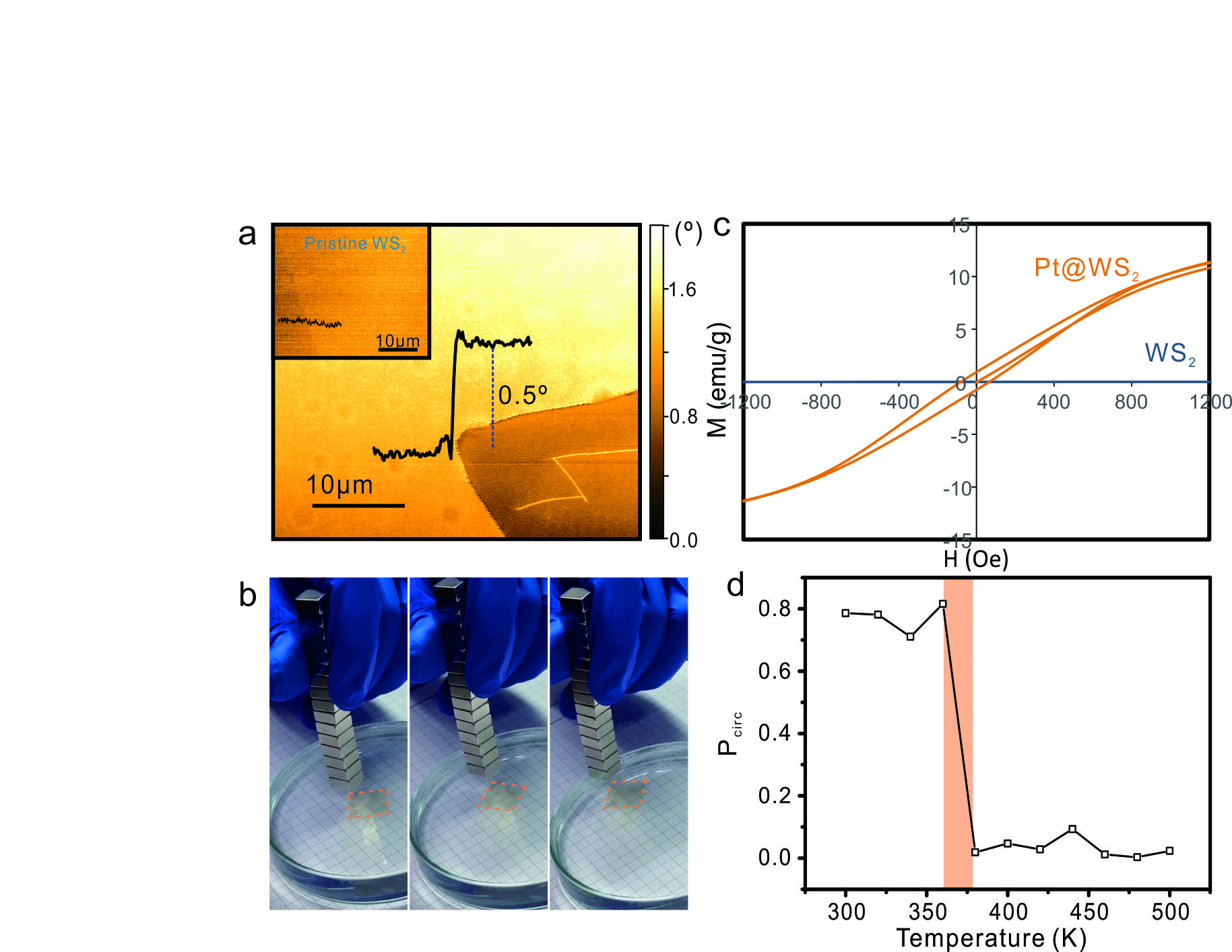
Extrinsic dilute magnetic semiconductors achieve magnetic functionality through
tailored interaction between a semiconducting matrix and a non-magnetic dopant. The absence
of intrinsic magnetic impurities makes this approach promising to investigate the newly
emerging field of two-dimensional dilute magnetic semiconductors. Here we demonstrate the
first realization of an extrinsic 2D DMS in Pt-doped WS2. A bottom-up synthesis approach
yields a uniform and highly crystalline monolayer where platinum selectively occupies the
tungsten sub-lattice. The orbital overlap between W 4d and Pt 5d results in a spin-selective
hybrid states that produce a strong valley-Zeeman splitting. Combined experimental and
theoretical results show that this interaction yields a sizable ferromagnetic response with a Curie
temperature around 375K. Our results open up a new route toward 2D magnetic properties
through tailoring of atomic interactions for future applications in spintronics and magnetic
nanoactuation.
Nano Letters 24, 1, 67 (2024)
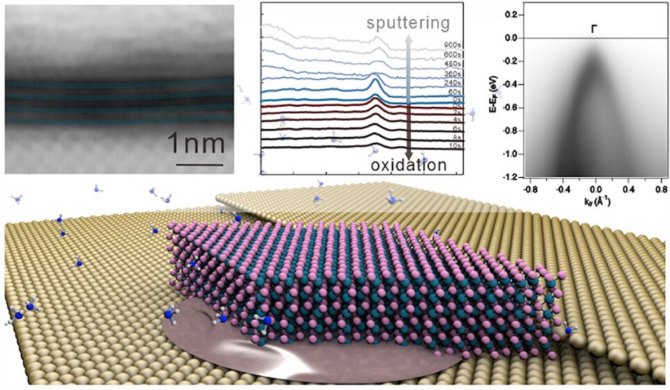
Two-dimensional transition metal nitrides offer intriguing possibilities for achieving novel electronic and mechanical functionality owing to their distinctive and tunable bonding characteristics compared to other 2D materials. We demonstrate here the enabling effects of strong bonding on the morphology and functionality of 2D tungsten nitrides. The employed bottom-up synthesis experienced a unique substrate stabilization effect beyond van-der-Waals epitaxy that favored W5N6 over lower metal nitrides. Comprehensive structural and electronic characterization reveals that monolayer W5N6 can be synthesized at large scale and shows semimetallic behavior with an intriguing indirect band structure. Moreover, the material exhibits exceptional resilience against mechanical damage and chemical reactions. Leveraging these electronic properties and robustness, we demonstrate the application of W5N6 as atomic-scale dry etch stops that allow the integration of high-performance 2D materials contacts. These findings highlight the potential of 2D transition metal nitrides for realizing advanced electronic devices and functional interfaces.
ACS Nano 18, 19828 (2024)
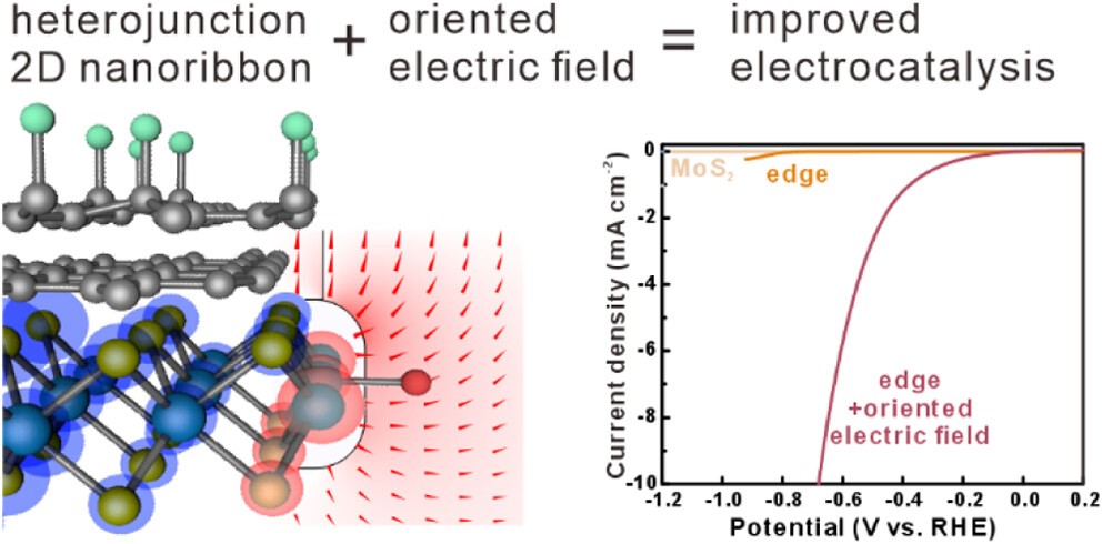
The edges of 2D materials have emerged as promising electrochemical catalyst systems, yet their performance still lags behind that of noble metals. Here, we demonstrate the potential of oriented electric fields (OEFs) to enhance the electrochemical activity of 2D materials edges. By atomically engineering the edge of a fluorographene/graphene/MoS2 heterojunction nanoribbon, strong and localized OEFs were realized as confirmed by simulations and spatially resolved spectroscopy. The observed fringing OEF results in an enhancement of the heterogeneous charge transfer rate between the edge and the electrolyte by 2 orders of magnitude according to impedance spectroscopy. Ab initio calculations indicate a field-induced decrease in the reactant adsorption energy as the origin of this improvement. We apply the OEF-enhanced edge reactivity to hydrogen evolution reactions (HER) and observe a significantly enhanced electrochemical performance, as evidenced by a 30% decrease in Tafel slope and a 3-fold enhanced turnover frequency. Our findings demonstrate the potential of OEFs for tailoring the catalytic properties of 2D material edges toward future complex reactions.
Hao-Ting Chin, Jiri Klimes, I-Fan Hu, Ding-Rui Chen, Hai-Thai Nguyen, Ting-Wei Chen, Shao-Wei Ma, Mario Hofmann, Chi-Te Liang & Ya-Ping Hsieh
Nature Communications, 12:6291 (2021).
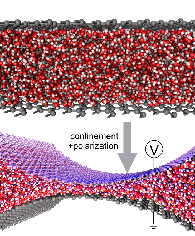
We here report on the direct observation of ferroelectric properties of water ice in its 2D phase. Upon nanoelectromechanical confinement between two graphene layers, water forms a 2D ice phase at room temperature that exhibits a strong and permanent dipole which depends on the previously applied field, representing clear evidence for ferroelectric ordering. Characterization of this permanent polarization with respect to varying water partial pressure and temperature reveals the importance of forming a monolayer of 2D ice for ferroelectric ordering which agrees with ab-initio and molecular dynamics simulations conducted. The observed robust ferroelectric properties of 2D ice enable novel nanoelectromechanical devices that exhibit memristive properties. A unique bipolar mechanical switching behavior is observed where previous charging history controls the transition voltage between low-resistance and high-resistance state. This advance enables the realization of rugged, non-volatile, mechanical memory exhibiting switching ratios of 106, 4 bit storage capabilities and no degradation after 10,000 switching cycles.
Ying-Yu Wang, Ding-Rui Chen, Jen-Kai Wu, Tian-Hsin Wang, Chiashain Chuang, Ssu-Yen Huang, Wen-Pin Hsieh, Mario Hofmann, Yuan-Huei Chang, Ya-Ping Hsieh*
Nano Lett., https://doi.org/10.1021/acs.nanolett.1c02331 (2021).
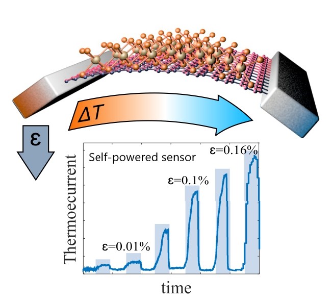
We here demonstrate the multifunctional properties of atomically thin heterojunctions that are enabled by strong interfacial interactions and their integration into ultra-high performance, self-powered sensors. Epitaxial alignment between tin diselenide and graphene through direct growth produces thermoelectric and mechanoelectric properties beyond the ability of either component. An unprecedented ZT of 2.43 originated from the synergistic combination of graphene’s high carrier conductivity and SnSe2 mediated thermal conductivity lowering. Moreover, strong interaction at the SnSe2/graphene interface produces stress localization that results in a novel 2D-crack-assisted strain sensing mechanism whose sensitivity (GF=450) is superior to all other 2D materials. Finally, the graphene-assisted growth process, permits the formation of high-quality heterojunctions directly on polymeric substrates for flexible and transparent self-powered sensors that achieve fast and reliable strain sensing from a small temperature gradient. Our work enhances the fundamental understanding of multifunctionality at the atomic scale and provide a route towards structural health monitoring through ubiquitous and smart devices.
Szu‐Hua Chen, Mario Hofmann, Zhi‐Long Yen, and Ya‐Ping Hsieh*
Advanced Functional Materials, 2004370 (2020).
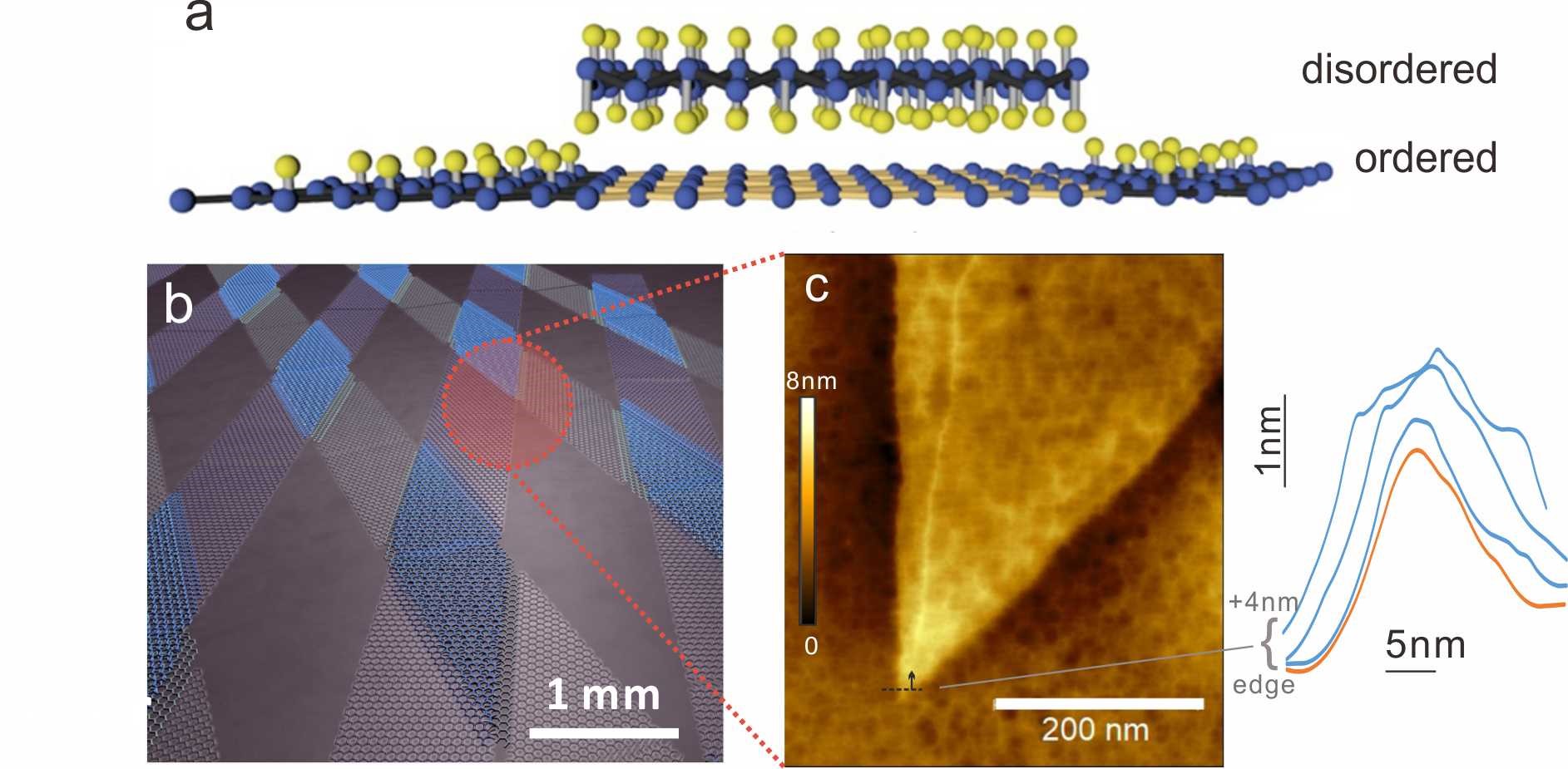
Atomic‐precision patterning at large scale is a central requirement for nanotechnology and future electronics that is hindered by the limitations of lithographical techniques. Historically, imperfections of the fabrication tools have been compensated by multi‐patterning using sequential lithography processes. The realization of nanometer‐scale features from much larger patterns through offset stacking of atomically thin masks is demonstrated. A unique mutual stabilization effect between two graphene layers produces atomically abrupt transitions that selectively expose single‐layer covered regions. Bilayer regions, on the other hand, protect the underlying substrate from removal for several hours permitting transfer of atomic thickness variations into lateral features in various semiconductors. Nanoscopic offsets between two 2D materials layers could be introduced through bottom‐up and top‐down approaches, opening up new routes for high‐resolution patterning. A self‐aligned templating approach yields nanometer‐wide bilayer graphene nanoribbons with macroscopic length that produces high‐aspect‐ratio silicon nanowalls. Moreover, offset‐transfer of lithographically patterned graphene layers enables multipatterning of large arrays of semiconductor features whose resolution is not limited by the employed lithography and could reach <10 nm feature size. The results open up a new route to combining design flexibility with unprecedented resolution at large scale.
